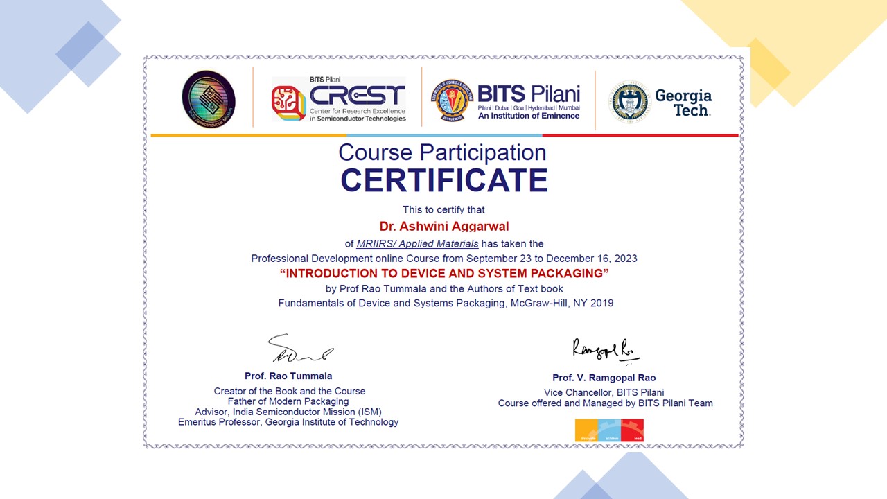
2 sessions per weekend; 1.5-2 hrs per session! + a range of exciting of tech talks on semiconductor packaging over the last 4 months earned me my Certification in Device and Systems Packaging from BITS Pilani/ Georgia Tech collaborative course.
What was more exciting in this journey was the fact that there were over 200 attendees who signed in for the online class – from academic faculty, students to industry practitioners. Clearly, the interest in India’s nascent semiconductor packaging industry prospects was high, driven by the India Semiconductor Mission’s aggressive incentives, progressive vision and interest by a range of global and Indian companies.
My interest was professional – to establish a foundation fo my professional work at Applied Materials. The course was really quite good and is strongly recommended for those who wish to understand and play in this sector. However, as I briefed in the concluding session, it could be enriched by adding more details on advanced semiconductor packaging manufacturing. The course focused on covering the advanced semiconductor packages but then only conventional semiconductor packaging was discussed.
Perhaps in future, the course will evolve to address the reality of the packaging industry – it is driven tightly by economics and markets. Already, Advanced Semiconductor Packaging is shifting the manufacturing economics with innovations like panel-level packaging that drive manufacturing costs/productivity shifts by an order of magnitude. Indeed, because of these shifts and other factors, Advanced Semiconductor Packaging is projected to evolve to more than 55% of the market by 2026! That is now the end of next year! (No longer that distant in future)!
Indeed, India players need to have a clear focus on their target markets in the cut-throat world of ATMP else they will get burnt badly.
Micron , of course, will have its global roadmap and India tactical strategy covering these evolutions; big players like Tata would have worked out an appropriate strategy as well. I am a little concerned on the smaller players who enter the market late just on the ISM incentive promise. The key is not just the incentive – it is the market!
If they start with the market, they cannot go wrong! The question is -are they?
In any case, we seem to be heading for an exciting period ahead – and definitely, 2024 is going to be an interesting, pivotal year in our efforts to develop India’s semiconductor manufacturing industry.
In the meantime, I am adding the following certification to my portfolio of technical qualifications:
AKA Certificate Device & System Packaging TR Dec23
For those of you who do want to get an overview of the semiconductor packaging industry – I recommend you go thru my post/video/lecture notes at the following links.
ATMP post
Semiconductor Packaging – Concepts & Practice – Primer (part 2/4) /ATMP Technology Global Markets
Finally, a thought for the road…