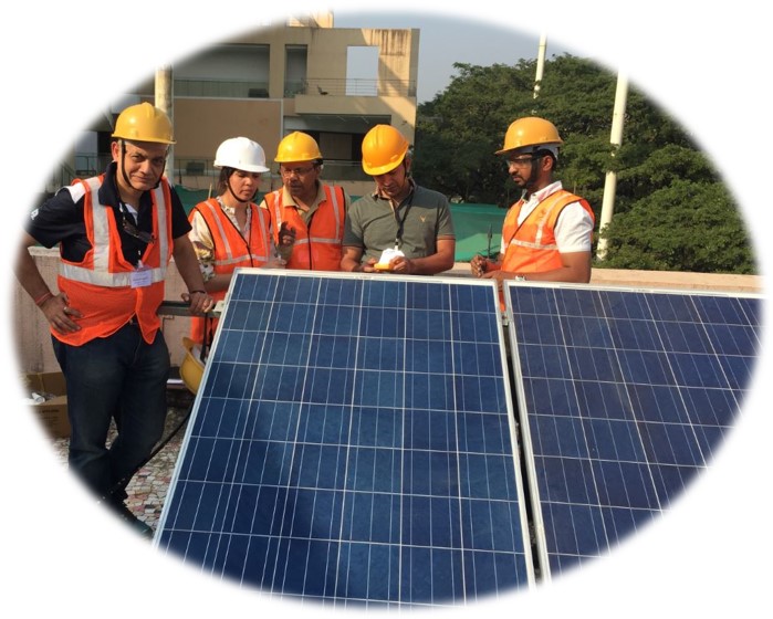
Dec 2nd: IEEE EPS DL by Dr Ram Achar, Carleton University. ( Flanked by Dr Umesh Dutta, CEO MRIIF and Dr Ashwini (self))!
The genesis of the IEEE EPS Delhi-NCR chapter was in the highly successful IEEE EPS events by the Bangalore chapter.
Kavita, Arun and Namita had done an excellent job of nurturing the Bangalore chapter and the ’22 and ’23 EPS events at Bangalore were a phenomenal service to the evolving semiconductor packaging industry in India.
Working with Prof Tummala Rao (Georgia Tech, Member Advisor- ISM) on the packaging initiatives as the Applied Materials lead for enabling government in its industry vision, I felt that there was a projected need emerging in North India. While Tata OSAT was in Assam (with a pilot plant in Hosur), CG Power and Kaynes Semiconductors had announced their projects for Gujarat. Micron was also in Gujarat.
Yet, North India was not a barren landscape for semiconductor packaging. Sahasra Semiconductors – the first commercial OSAT in India- was based out of ELCINA cluster, Bhiwadi in Delhi NCR area (about 1.5 hr. drive from my place). SCL Chandigarh, India’s fab lab, and proof point that defied the naysayers with chips that powered India’s space program was 4 hours from Delhi. CDIL had activated its SiC device packaging line at Chandigarh as well. IDEMIA, the world’s largest smart card manufacturer, is packaging 66 crore smart cards a year at its Noida plant. The ATMP for that was fed by ~700 imported 300mm wafers/month and this facility was also operational from Aug’23. Sahasra Semiconductors had its commercial production start in Feb’23 and its IPO earlier this year was a resounding success. Clearly, their project would grow with multiple lines and advanced technology now that capital had been successfully raised and the founders’ vision and morale was at its peak.
The government has also announced a major investment plan to reinvigorate SCL operations! Then there are the Expressions-of-interests which will likely get an impetus post the Feb’25 budget and announcement of ISM 2.0. India Semiconductor Mission is expected to get a fresh infusion of funds to continue to expand the Indian semiconductor ecosystem. Tarq Semiconductors (Hiranandani group) has announced a GaN project with Transform/ Renesas as the technology provider; Vamasundari (a HCL – Foxconn) initiative is cleared by UP Government for an OSAT project – and PM Modi has announced a niche initiative of 3rd I-tech in the Wide Band Gap Semiconductor space. Interestingly, these 3 projects are all targeting the Yamuna Expressway near Jewar airport (expected to be ~35 min drive from my place in Faridabad on the new highway)!
The regional investments apart, there is a strong talent pool in North India with multiple institutes (IIT Delhi, Mandi, Jodhpur, Kanpur); CEERI Pilani having their own fab labs. CEERI, Pilani was the fountain head DSIR lab that pioneered the semiconductor initiative in India. It has a fairly comprehensive process capability and has demonstrated several breakthrough tech capabilities in semiconductors and LED technologies.
In Feb’24, at ISPECS Chandigarh, I discussed the thought of creating an IEEE EPS Delhi-NCR chapter with Dr Ravi Mahajan, Intel and IEEE Fellow. Ravi’s encouragement and support led me to filing the petition for IEEE EPS Delhi Chapter. I was supported by Dr Rishu Chaujjar, Center head for Vinod Dham Center of Excellence at Delhi Tech University, Dr Anuj Grover, IIIT Delhi and Dr Umesh Dutta, Manav Rachna International Institute of Research & Studies Faridabad. Industry support came from Yogesh Adalatwale at ELCINA. Ravi’s mentorship and support made all the difference as I negotiated the IEEE processes, explained that Faridabad, Gurgaon, Noida were all suburbs of Delhi – just like SFO had suburbs in the Bay area! Denise Manning at IEEE EPS WW office helped process the petition thru which became a reality in July. With my retiral in July and SEMICON India in September, I executed a phenomenally successful training on Semiconductor Manufacturing skills at IIT Delhi on September 9. However, we could not register it as an IEEE event as I was fully loaded with the SEMICON activities.
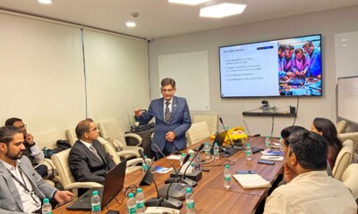
2nd December IEEE EPS Workshop with a Tech Talk by IEEE Distinguished Speaker, Dr Ram Achar, from Carleton University, Canada is therefore the formal kickoff for the IEEE-EPS Delhi NCR chapter. Dr Ram Achar’s talk focused on the challenges to signal integrity as the geometries shrunk and the effect of chip and package parasitic signals, crosstalk and high frequency signals compounded. Dr Ram also adapted his presentation to address the evolving needs of workforce development in India and shared how Carleton University could extend its semiconductor lab facilities to give a hands-on, design to tape-out exposure to Indian students in short 4–6-week courses.
Dr Priyadarshini Ghosh, Application Specialist, at Horiba presented the company’s seminal products servicing the global semiconductor industry. Horiba is a Japanese MNC but has a strong base in India with multiple sites including manufacturing at Haridwar, Pune and offices across India. Their precision Mass Flow Controllers are the defacto standard in the highly demanding Semiconductor sector. In fact, Horiba is a key supplier for Applied Materials Equipment tools worldwide. Equally interestingly, their characterization tools (Nano-Raman Spectroscopy from HORIBA is again a global Tech leader product) and tools for Semiconductor grade Ultra-Pure, DI Water characterization are key for the semiconductor sector.
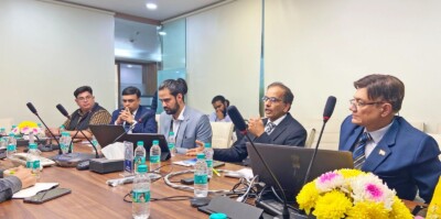
I presented briefly on the work being done by the Manufacturing Skill Development group under Prof Tummala Rao leadership- a detailed deep dive into a job role would be the topic of a future webinar in December. On behalf of the ~20 in-person participants and 3 virtual participants, I specifically thank Salim Ahmad, Acting COO and Varun Bhatia at Electronics Sector Skill Council of India for hosting the event. Earlier this year, we struggled to get 12 members to complete the IEEE EPS petition. Now – We have 45 members in the North, ~20 in Delhi NCR region. – Dr Rakhi Nangia, IESA , is looking at leveraging Carleton connect in IESA Talent Program – Webinar on Wafer Dicing is planned in end December – Manav Rachna is looking at hosting the IEEE EPS Delhi NCR conference in end March.
BTW- we have followed up the Dec 2nd event with another event – a webinar on Dec 23rd featuring the Semiconductor Manufacturing Skills for Wafer Dicing in the conventional packaging process flow!
Despite an examination season, we had a decent participation, and I think the ship has sailed!