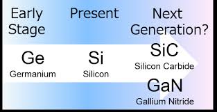
With Govt of India (Ministry of Electronics & IT) giving another call for an Expression of Interest for Semiconductor Fab, there is a keen interest in select players for exploring a WBG semiconductor fab.
On behalf of Applied Materials and ELCINA, I have been conducting a series of Semiconductor Manufacturing workshops addressing Government and Industry Stakeholders and covering a range of topics from CMOS Silicon technologies, to Advanced Packaging and ATMP at the backend and , recently , the Wide Band Gap Semiconductors.
Wide-Band Gap Semiconductors are expected to be a few Bln $ opportunity by servicing applications in Power electronics and RF devices with their promise of bringing an overall system size reduction at given or better performance levels. With GaN based chargers entering mainstream consumer market radar in 2019-20, there is a rapid increase in GaN revenue! Combined SiC and GaN power devices market is around $800mln – and expected to cross $2bln by 2024!
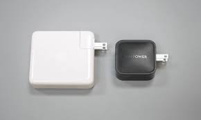
As shared in the image below, the GaN chargers can deliver functional advantages like significant ( ~50%) size reduction, better thermal properties at given breakdown voltages.
While SiC devices are ideal for voltage levels from 600V and above, GaN devices can play between 40->600 V, and while there is a battlefield at the interim point, by-and-large each device category has its own market footprint.
Historically, the defect density in the GaN crystal has been very high and has only been tamed to some extent in the recent years. Another challenge is the lattice match between the WBG layer wrt the base substrate. GaN on SiC is a good match – but higher costs. On the other hand, GaN on Si has a poor match and results in issues like warpage, film defects though it leverages the Si technology costs! These challenges also mean that the WBG devices mostly get manufactured on lower sized wafer coupons – 4” and 6” wafer coupon is quite common and 8” wafer is emerging on the horizon. On the other hand, this also means that the WBG semiconductor fab can be realized at lower Capex cost!
Attached is my presentation deck from the WBG workshop.
Semiconductors – Primer WBG 3 Ext Mar21
The full video recording of the WBG Semiconductor Primer workshop is shared.
You can also access a very nice GaN manufacturing video from EPC here.
Dr. Francois Short Bio from SiCamore Semi, USA joined me in evangelizing the potential of SiC semiconductor devices. You can access his presentation here.
WBG Overview AMAT India March 25 2021 Michele
You can also view the previous semiconductor primer workshop contents at the following posts:
Semiconductor Packaging – an industry Primer
Semiconductors- an industry primer
I do hope to plan a primer on Analog devices/ MEMS and another on Display Fab in future. If you have any suggestions for future content, please leave a note in the comments – and subscribe below for future alerts!
2 Responses
Vishal Srivastava
Dear Sir,
We are please let us know how a micro enterprise can do the manufacturing of semiconductor if they know and have the expertise to do it, but we are lacking in support of funds and infrastructure.
Regards
Ashwini Aggarwal
Dear Vishal
A typical GaN fab could be an investment running into a few hundred crores + you will need a lot of working capital to manufacture – and then a lot of marketing muscle to move the chips into the market. I would not recommend it as an activity for a micro-enterprise in India at this stage. I do believe that government may precipitate a GaN proto fab that will serve as an incubation engine in this area. Let us hope that vision is actualized …
Warm Regards
Ashwini