

Top Stories

Received my earned MTech Degree at MRIIRS yesterday! There was no concept of a convocation in St Stephens for BSc


Recent Stories
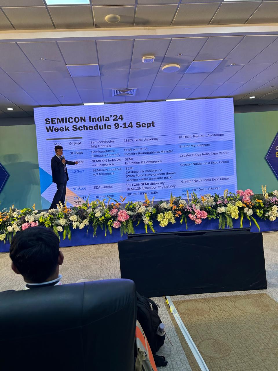
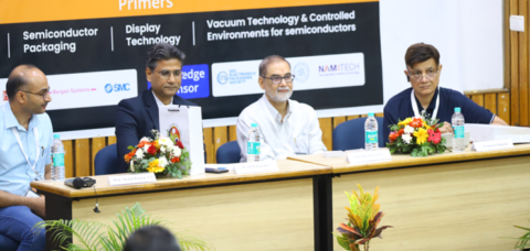
My keynote presentation at Gujarat Semiconnect 24 earlier this week explored the issues in "Developing India's Semiconductor Manufacturing Workforce" and was based on the following principles: Semiconductor Manufacturing skills are different from design skills. India has its design industry, but

I was just informed that I have been elevated to IEEE Senior Member. This is an honor bestowed only to those who have made significant contributions to the profession. In my case, I believe it was my work at Electronics

The PhD journey is a demanding one - with a lot of ups and downs! Feeling pulled down?! Take this tip!!

In June 1st week, I completed my MTech in ECE with specialization in Semiconductors, VLSI and Embedded System Design. Nelson Mandela has said that education is the single most powerful tool for changing the world. I know that it has been

What is there in the chamber when everything is taken out of it? Nothing! ...or Vacuum!! Vacuum technology is fundamental to Semiconductors manufacturing! A fab process engineer should have a strong understanding of vacuum technology as most chambers have

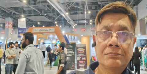
( In the picture: Sonny Kunnakat, MD Worldwide Operations Applied Materials with Honble Minister, Ashwini Vaishnaw. Also present, CEO ISM Akash Tripathi ji, Chief of Staff-ISM Sagar Sharma and Shannu Kaw Sr Director, Applied Materials) Led a door-knock session for